Search any question & find its solution
Question:
Answered & Verified by Expert
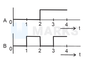
For the logic circuit shown, the output waveform at is

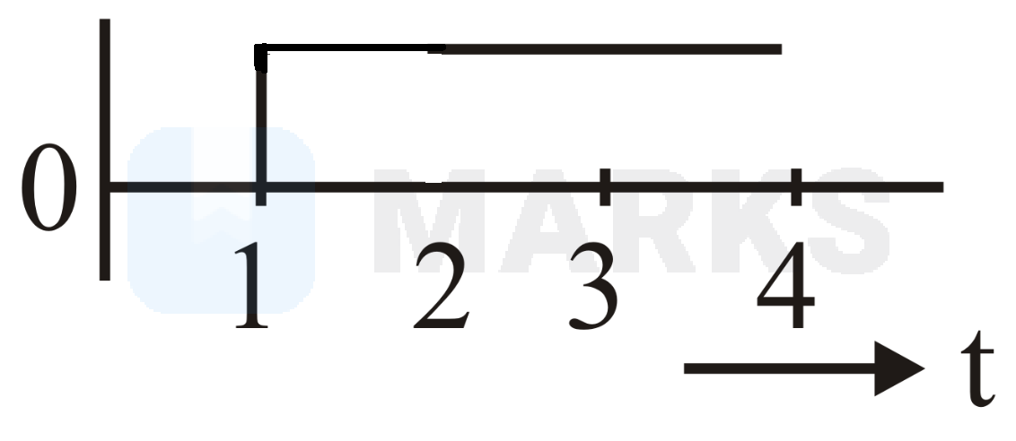
- A
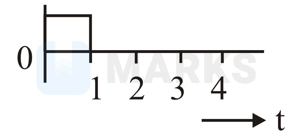
- B

- C
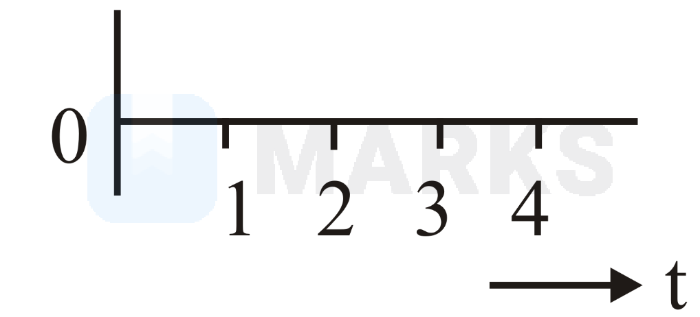
- D
Solution:
2869 Upvotes
Verified Answer
The correct answer is:
All the gates used in the diagram represent NAND gates.
Thus, the output can be calculated as follows
The above equation suggests that the output of the given combination yields the same result as an OR gate.
The truth table can be written as follows
Hence, this is the correct output.
Looking for more such questions to practice?
Download the MARKS App - The ultimate prep app for IIT JEE & NEET with chapter-wise PYQs, revision notes, formula sheets, custom tests & much more.