Search any question & find its solution
Question:
Answered & Verified by Expert
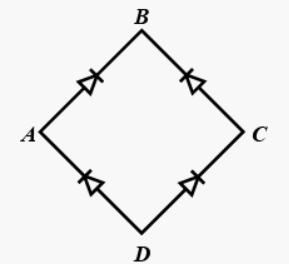
In the diagram, the input is across the terminals $A$ and $C$ and the output is across the terminals $B$ and $D$, then the output is
Options:
Solution:
2345 Upvotes
Verified Answer
The correct answer is:
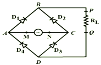
Full wave rectifier
During half cycle when $\mathrm{V}_{\mathrm{M}} \gt \mathrm{V}_{\mathrm{N}}, \mathrm{D}_1$ andD $\mathrm{D}_3$ are forward biased. The path of current is MABPQDCNM. In second half cycle, $V_N\gtV_M, D_2$ and $D_4$ are forward biased while $D_1$ and $D_3$ are reverse biased. Hence, path of current is, NCBPQDAMN.
Therefore, in both half cycles, current flows from P toQ from load resistance $R_L$. It is full wave rectifier.
Therefore, in both half cycles, current flows from P toQ from load resistance $R_L$. It is full wave rectifier.
Looking for more such questions to practice?
Download the MARKS App - The ultimate prep app for IIT JEE & NEET with chapter-wise PYQs, revision notes, formula sheets, custom tests & much more.